


 Global Sourcing Spotlight: Golf, Friedman, and the Benefits of Global Sourcing
 Nolan’s Notes: Coming to Terms With AI
 The Knowledge Base: A CM’s Perspective on Box Build Practices
Overview Miniaturization on Large Form Factor PCBA
February 24, 2016 | D. Geiger, A. Mohammed, M. Kurwa, AEG, Flextronics International Inc.Estimated reading time: 10 minutes
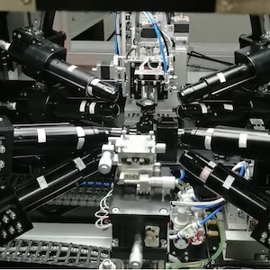
Figure 3: Various configurations.
This ability to maintain the adjacent component temperatures below the can allow the BGA to IC components to be placed closer together in the designs. Further advances in rework technology will need to be pursued in order to help drive the component spacing down further. Most techniques today require some sort of fixturing in order to protect or have nozzles surround the device being reworked. Laser, Vapor Phase and other techniques are being explored to help move this technology even further.
For the passive components a lot of research has been done to place these components very close together. In consumer/miniaturized products the component to component spacing is down to 0.150mm and in some cases down to 0.100mm in limited areas. Picture 2 shows a spacing matrix of 0.125mm between 01005 and 0201 style capacitors.
In these cases printing is a key item to achieve good yields. In Figure 4 below it shows the yield of the various spacing vs the stencil thickness being used. A thinner stencil helps create a higher yield however at 0.250mm spacing good yields can be seen for the stencil thicknesses in the study.
Figure 4: DPMO vs component Spacing vs Stencil thickness.
For larger form factor boards, components down to 0402 can still utilize a 125µm thick stencil and still achieve component to component spacing down to 0.250µm in localized areas.
Figure 5: 0402 vs 0201 vs 01005 space taken.
Some of the other key issues to be aware of is the placement sequences. In order to place the parts close together, the placement sequence needs to be able to place the shortest components first followed by the next shortest working the way up to the tallest components. This will help prevent the placement nozzle from disturbing the placement of the component already placed on the PCBA.
Finer pitch components
One last way higher density on a PCB can be obtained is through the use of components with finer pitch. Today the use of 0.4mm pitch bottom terminated components and chip scale packages are being used on the larger format boards. One reason they are being used has to do with the availability of these types of components. The consumer (smart phones and others) are using a large volume of the components such as memory which are also desirable to be used in server, storage and other infrastructure types of products. The same concens exist on these finer pitches that currently have been discussed and that is the ability to print these fine pitches consistently. Moving to the thinner stencil help alleviate this concern and allows good consistent printing of solder paste to be able to be done.
Along with finer pitch components some designs want to use the package on package (PoP, Picture 3) technology where the packages are stacked during the SMT process. This process has been around for 10 years and is well understood.
The key factors are the component warpage and the use of nitrogen in reflows to minimize the potential for open solder joints. One of the limiting factors is the lack of inspection techniques for these stacked solder joints. Current automated x-ray inspection systems are limited in the capability to inspect solder joints on a separate z plane. However, work is being done to address these issues. Inspection is a key element in the process to help ensure that the solder joints are robust for the long term reliability that the larger form factor products usually will have.
Another concern for the fine pitch process is the printed circuit board itself. With the unpredictable shrinkage of the PCBs, this can cause issues with the printing due to alignment of the stencil to the PCB. The stencil is typically made to the gerber and not adjusted for any shrinkage of the PCB after baking or reflow. The amount of shrinkage can cause the board pads to no longer align to the stencil apertures. One way this is overcome is by creating a stencil based on the batch of PCB received and adjusting the fabrication of the stencil to match those PCBs. The pick and place can make adjustments to the x,y position based on the fiducials and apply a scaling. The stencils do not have this ability as they are fixed and the only alignment that can be done is to create a best fit location based on fiducials. In some cases the outer components can be misaligned in the stencil print process.
Page 2 of 3
Share on:


Suggested Items
Connect the Dots: Designing for Reality—The Pre-Manufacturing Process
05/08/2024 | Matt Stevenson -- Column: Connect the DotsI have been working with Nolan Johnson on a podcast series about designing PCBs for the reality of manufacturing. By sharing lessons learned over a long career in the PCB industry, we hope to shorten learning curves and help designers produce better boards with less hassle and rework. Episode 2 deals with the electronic pre-manufacturing process. Moving from CAD (computer-aided design) to CAM (computer-aided manufacturing) is a key step in PCB manufacturing. CAM turns digital designs into instructions that machines can use to actually build the PCB.
AIM Solder Signs Shinil Fl Ltd. as New Distributor for Korea
05/08/2024 | AIM SolderAIM Solder, a leading global manufacturer of solder assembly materials for the electronics industry, is pleased to announce a new distribution partnership with Shinil Fl Ltd., a prominent supplier of technological solutions in the SMT and semiconductor sectors.
Indium Corporation to Showcase HIA Materials at ECTC
05/07/2024 | Indium CorporationAs an industry leader in innovative materials solutions for semiconductor packaging and assembly, Indium Corporation® will feature its advanced products designed to meet the evolving challenges of heterogeneous integration and assembly (HIA) and fine-pitch system-in-package (SiP) applications at the 74th Electronic Components and Technology Conference (ECTC), May 28‒31, in Denver, Colorado.
Indium Corporation Expert to Present on Pb-Free Solder for Die-Attach in Discrete Power Applications
04/30/2024 | Indium CorporationIndium Corporation Product Manager – Semiconductor Dean Payne will present at the Advanced Packaging for Power Electronics conference, hosted by IMAPS, held May 8-9 in Woburn, Massachusetts, USA.
Taiyo Circuit Automation Installs New DP3500 into Fuba Printed Circuits, Tunisia
04/25/2024 | Taiyo Circuit AutomationTaiyo Circuit Automation is proud to be partnered with Fuba Printed Circuits, Tunisia part of the OneTech Group of companies, a leading printed circuit board manufacturer based out of Bizerte, Tunisia, on their first installation of Taiyo Circuit Automation DP3500 coater.